Field effect transistor
Large power N-channel field effect transistor
Terminals
All FET's, except J-FET's, have four terminals, which are known as the gate, drain, source and body/base/bulk. Compare these to the terms used for BJTs: base, collector and emitter. BJT's and J-FET's have no body. It is common in large FET's to connect the body and source internally to simplify design. In most applications one would connect the source to the body anyway. The voltage applied between the gate and source terminals modulates the current between the source and drain terminals. A difference between the voltages of the source and body will change the threshold voltage. This is known as the body effect and is used primarily in digital circuits, although it is taken into effect in high precision analog circuits. There are two 'modes' of FET: enhancement, in which a voltage applied to the gate increases the current flow from source to drain; and depletion, in which a voltage applied decreases the current flow from source to drain. Thus enhancement FETs are normally off, whereas depletion FETs are normally on.
Composition
Most FETs are made with conventional bulk semiconductor processing techniques, using the single crystal semiconductor wafer as the active region, or channel.
Types of field-effect transistors
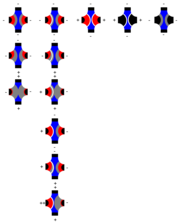
Depletion type FETs under typical voltages. JFET, poly-silicon MOSFET, double gate MOSFET, metal gate MOSFET, MESFET. depletion , electrons, holes, metal, insulator . Top=source, bottom=drain, left=gate, right=bulk. Voltages the lead to channel formation are not shown
The FET is simpler in concept than the bipolar transistor and can be constructed from a wide range of materials. The channel region of any FET is either doped to produce n-type semiconductor, giving an "N-channel" device, or with p-type to give a "P-channel" device. The doping determines the polarity of gate operation. The different types of field-effect transistors can be distinguished by the method of insulation between channel and gate:
Among the more unusual body materials are amorphous silicon, polycrystalline silicon or other amorphous semiconductors in thin-film transistors or organic field effect transistors that are based on organic semiconductors and often apply organic gate insulators and electrodes.
FET Operation
The shape of the conducting channel in a FET is altered when a potential difference is applied to the gate terminal (potential relative to either source or drain.) In an n-channel "depletion-mode" device, a negative gate voltage causes a depletion region to expand in size and encroach on the channel from the side, narrowing the channel. If the depletion region completely closes the channel, the resistance of the channel becomes very large, and the FET is effectively turned off. Positive gate voltage attracts electrons from the surrounding semiconductor next to the gate, forming a conductive channel. At low source-to-drain voltages, small changes to the gate voltage will alter the channel resistance. In this mode the FET operates like a variable resistor. This mode is not employed when amplification is needed.
If a larger potential difference is applied between the source and drain terminals, this creates a significant current in the channel and produces a gradient of potential from source to drain. This also causes the shape of the depletion region to become asymmetrical–one end of the channel becomes narrow. If the potential difference is large enough, the depletion region begins to close the channel. The FET is said to be in saturation. Rather than entirely blocking the electrons from flowing from source to drain, electrons flow through the depletion region in a controlled manner. Any attempted increase of the drain-to-source voltage will lengthen the depletion region, increasing the channel resistance proportionally with the applied drain-to-source voltage which causes the value of drain current to remain relatively fixed. This mode of operation is called pinch-off. In this mode, the FET behaves as a constant-current source rather than as a resistor and can be used as a voltage amplifier. The value of gate voltage determines the value of the constant current in the channel.
An "enhancement-mode" device is of slightly more complex construction. Rather than only being one material, it is made of a three-piece sandwich: similar to either an npn or a pnp transistor with no base connection, but still with a gate. In this case, the device is "normally-off" since one of the two junctions will always be reverse biased. The npn device is called an n-channel device and the pnp device is called a p-channel device.
Uses
The most commonly used FET is the MOSFET. The CMOS (complementary-symmetry metal oxide semiconductor) process technology is the basis for modern digital integrated circuits. This process technology uses an arrangement where the (usually "enhancement-mode") p-channel MOSFET and n-channel MOSFET are connected in series such that when one is on, the other is off. In CMOS logic devices, the p-channel device pulls up the output and the n-channel device pulls down the output. The great advantage of CMOS circuits is that they allow no current to flow (ideally), except during the transition from one state to the other, which is very short. The gates are capacitive, and the charging and discharging of the gates each time a transistor switches states is the primary source of power usage in fast CMOS logic circuits.
The fragile insulating layer of the MOSFET between the gate and channel makes it vulnerable to electrostatic damage during handling. This is not usually a problem after the device has been installed.
FETs can switch signals of either polarity on the source or drain terminals, if their amplitude is significantly less than the gate swing, as the devices are typically symmetrical. This makes FETs suitable for switching analog signals between paths (multiplexing). With this concept, one can construct a solid-state mixing board, for example.
The power MOSFET has a reverse-biased 'parasitic diode' shunting the conduction channel that has half the current capacity of the conduction channel. Sometimes this diode is used when driving inductive circuits, but in other cases it causes problems.
A more recent device for power control is the insulated-gate bipolar transistor, or IGBT. This has a control structure akin to a MOSFET coupled with a bipolar-like main conduction channel. These have become quite popular in the 200-3000 V range of operation, as they overcome limitations of Power MOSFET in high voltage. Power MOSFETs are still the device of choice (and practically the only choice available) for low voltage (from less than 1 V to 200 V) applications.